LTC4224-1/LTC4224-2
7
422412fa
APPLICATIONS INFORMATION
V
CC
Selection
The LTC4224 is powered from the higher of its two supply
pins, V
CC1
and V
CC2
.This allows the part to control a sup-
ply voltage as low as 1V , while the other supply is 2.7V or
greater. If both supplies are tied together, the part derives
its power from both equally. The Functional Diagram shows
the V
CC
selection circuit in an ideal diode OR-ing arrange-
ment. It is designed to ensure swift and smooth internal
power switchover from one supply to the other.
Turn-On Sequence
Separate ON1 and ON2 pins allow the V
CC1
and V
CC2
supplies to be turned on in any order. The power supplies
delivered to a plug-in card are controlled by external N-
channel MOSFETs, Q1 and Q2. For X2/XENPAK de ned
optical transceiver modules, it has been speci ed that the
MOD DETECT pin pulls low inside the module through a
1k resistor (R
MOD_DET
), as shown in Figure 1. Several
conditions must be satis ed to turn on the MOSFETs.
First, V
CC1
or V
CC2
must exceed the 2.4V V
CC
undervoltage
lockout level for longer than an internal UV turn-on delay
of 160ms. Next, if V
CCn
is greater than 0.8V and ONn is
low (<0.8V), a debounce delay of 10ms is started. If V
CCn
drops below 0.8V or ONn goes high before the end of the
10ms debounce delay, the debounce delay is restarted the
next time these pins are properly conditioned.
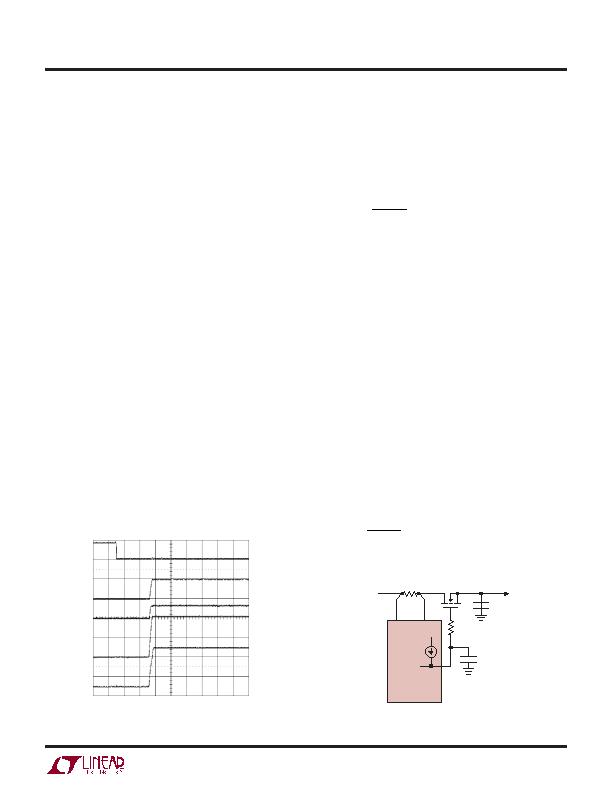
When the 10ms debounce delay expires, the external
MOSFET is turned on by charging up the GATE with a
Figure 2. Normal Power-Up Sequence
V
OUT1
5V/DIV
V
OUT2
5V/DIV
5ms/DIV
422412 F02
ON1/2
2V/DIV
GATE1
5V/DIV
GATE2
5V/DIV
10糀 charge pump generated current source. When the
GATE voltage reaches the MOSFET threshold voltage, the
inrush current can build up quickly as the GATE continues
to rise. The ACL ampli er actively controls the gate volt-
age to maintain 25mV across the sense resistor. In this
condition, the inrush current is given by:
I
INRUSH
=
25mV
R
SENSE
As the inrush current charges up the load capacitor, the
output rises with a corresponding increase in gate voltage.
When the supply is no longer in current limit, an internal
charge pump pulls the gate to 5.5V above the higher of V
CC1
or V
CC2
to achieve a low resistance power path. Figure 2
shows a typical start-up sequence with C
LOAD1
= C
LOAD2
= 150糉 , R
LOAD1
= 4.7?and R
LOAD2
= 2?
The inrush current can be reduced to below the current
limit level by adding an external gate capacitor as shown
in Figure 3.
GATE capacitor C
GATE
provides gate slew rate control to limit
the inrush current. However, C
GATE
could cause parasitic
high frequency self oscillation in Q1. A 10?resistor, R
G
, as
shown in Figure 3 can be used to prevent the oscillation.
To be effective, R
G
needs to be laid out close to Q1.
The voltage at the GATE pin rises with a slope equal to I
GATE
/
C
GATE
. For a given supply inrush current I
INRUSH
and load
capacitor C
LOAD
, C
GATE
can be calculated according to:
C
GATE
=
I
GATE
I
INRUSH
"C
LOAD
Figure 3. Inrush Current Control by Gate Capacitor
422412 F03
LTC4224
V
CC1
SENSE1
GATE1
R1
0.015?/DIV>
5V
I
GATE
C
GATE
R
G
10?/DIV>
C
LOAD
Q1
发布紧急采购,3分钟左右您将得到回复。
相关PDF资料
LTC4225IGN-1#PBF
IC CONTROLLER HOT SWAP 24-SSOP
LTC4230CGN#TRPBF
IC CONTRLLR HOT SWAP TRPL 20SSOP
LTC4232CDHC#TRPBF
IC CTLR HOT SWAP 5A 16-DFN
LTC4240IGN#TRPBF
IC CTRLR HOTSWAP CPCI I2C 28SSOP
LTC4241IGN#PBF
IC CTRLR HOTSWAP 3.3V AUX 20SSOP
LTC4242CUHF#TRPBF
IC CNTRLR HOT SWAP 38-QFN
LTC4244CGN-1#TRPBF
IC CTRLR HOTSWAP PCI 20-SSOP
LTC4245CG#TRPBF
IC CNTRLR HOT SWAP 36-SSOP
相关代理商/技术参数
LTC4224IDDB-2-PBF
制造商:LINER 制造商全称:Linear Technology 功能描述:Compact Dual Low Voltage Hot Swap Controller
LTC4224IDDB-2-TRPBF
制造商:LINER 制造商全称:Linear Technology 功能描述:Compact Dual Low Voltage Hot Swap Controller
LTC4224IMS-1#PBF
功能描述:IC CTLR HOT SWAP DUAL LV 10MSOP RoHS:是 类别:集成电路 (IC) >> PMIC - 热交换 系列:- 产品培训模块:Obsolescence Mitigation Program 标准包装:100 系列:- 类型:热插拔开关 应用:通用 内部开关:是 电流限制:可调 电源电压:9 V ~ 13.2 V 工作温度:-40°C ~ 150°C 安装类型:表面贴装 封装/外壳:10-WFDFN 裸露焊盘 供应商设备封装:10-TDFN-EP(3x3) 包装:管件
LTC4224IMS-1#TRPBF
功能描述:IC CNTRLR HOT SWAP DUAL 10-MSOP RoHS:是 类别:集成电路 (IC) >> PMIC - 热交换 系列:- 产品培训模块:Obsolescence Mitigation Program 标准包装:100 系列:- 类型:热插拔开关 应用:通用 内部开关:是 电流限制:可调 电源电压:9 V ~ 13.2 V 工作温度:-40°C ~ 150°C 安装类型:表面贴装 封装/外壳:10-WFDFN 裸露焊盘 供应商设备封装:10-TDFN-EP(3x3) 包装:管件
LTC4224IMS-1-PBF
制造商:LINER 制造商全称:Linear Technology 功能描述:Compact Dual Low Voltage Hot Swap Controller
LTC4224IMS-1-TRPBF
制造商:LINER 制造商全称:Linear Technology 功能描述:Compact Dual Low Voltage Hot Swap Controller
LTC4224IMS-2#PBF
功能描述:IC CNTRLR HOT SWAP DUAL 10-MSOP RoHS:是 类别:集成电路 (IC) >> PMIC - 热交换 系列:- 产品培训模块:Obsolescence Mitigation Program 标准包装:100 系列:- 类型:热插拔开关 应用:通用 内部开关:是 电流限制:可调 电源电压:9 V ~ 13.2 V 工作温度:-40°C ~ 150°C 安装类型:表面贴装 封装/外壳:10-WFDFN 裸露焊盘 供应商设备封装:10-TDFN-EP(3x3) 包装:管件
LTC4224IMS-2#TRPBF
功能描述:IC CNTRLR HOT SWAP DUAL 10-MSOP RoHS:是 类别:集成电路 (IC) >> PMIC - 热交换 系列:- 产品培训模块:Obsolescence Mitigation Program 标准包装:100 系列:- 类型:热插拔开关 应用:通用 内部开关:是 电流限制:可调 电源电压:9 V ~ 13.2 V 工作温度:-40°C ~ 150°C 安装类型:表面贴装 封装/外壳:10-WFDFN 裸露焊盘 供应商设备封装:10-TDFN-EP(3x3) 包装:管件